FET Buffer Deviation Calculator
Field effect transistors (FETs) are mainly composed of junction field effect transistors (JFETs) and insulated gate field effect transistors (MOS transistors). The field effect transistor is mainly composed of a majority of carriers, also known as unipolar transistors. Field effect transistor (FET) is a kind of semiconductor device which controls the output circuit current by controlling the electric field effect of the input circuit.
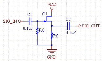
The following is a JFET buffer (common drain amplifier), useful in everyday use because it has a very high input impedance compared to transistors.
|
Equations: IDS= IDSS(1-VGS/Vp)2 RS= VRS/IDS VGS is called gate to source interleave voltage or cut-off voltage, which is shown by VGS (off). The case of N channel JFET is VGS (off). Value with negative symbols, measure the actual JFET corresponding ID = 0 VGS because it is very difficult, in the use of small signal JFET amplifier, will reach ID = 0.1-10muA VGS There are more cases defined as VGS (off). |